Take advantage of robust permanent bonding at low temperature for an unprecedented variety of materials.
It's easy — combine Impulse Current Bonding hardware with SB8 Gen2.
SB8 Gen2 Wafer Bonder
With the SB8 Gen2 Wafer Bonder SUSS MicroTec provides a semi-automated platform for multiple bonding processes. Handling wafers up to 200 mm as well as various shapes and types of substrates the SB8 Gen2 presents itself as a flexible tool for various applications and process environments. The SB8 Gen2 is suitable for packaging as well as structuring, meeting the requirements for MEMS, LED, advanced packaging, 2.5D integration, and 3D integration. more…
Due to high interatomic diffusion at the material interface, Impulse Current Bonding offers the advantage of bonding glass to silicon at temperatures as low as 180°C. Process temperatures below 200°C can also be attained for market-relevant non-silicon substrate materials like sapphire, lithium niobate/tantalate, silicon carbide etc.
Impulse Current Bonding combines the robustness of Anodic Bonding with the material versatility of other, more complex bonding methods. As a breakthrough in field-assisted bonding, ICB can successfully bond materials featuring large differences in CTE (coefficients of thermal expansion), such as glass to GaAs, and even alkali-free glass to silicon.

Glass bonded to Sapphire (with PVD layer)
Temperature: 200 °C
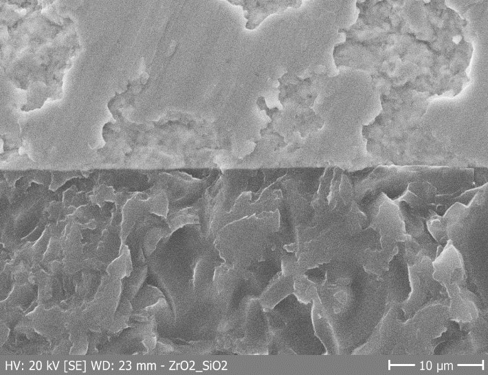
ZrO2 bonded to Glass
Temperature: 180 °C

SiC (with PVD layer) bonded to Glass
Temperature: 200 °C
High migration density leads to a strong and durable bond even at low temperatures. The interface created has a strength which exceeds that of the used bulk materials.
Compared to other direct bonding methods, Impulse Current Bonding is less susceptible to surface imperfections for achieving a high quality bond. Therefore, it does not require cost-intensive and often challenging surface conditioning steps such as chemical-mechanical polishing (CMP) and plasma treatment.
Besides the reduced need for surface preparation, the high migration density and low temperature lead to shorter process cycle times and significantly reduce overall energy consumption and cost per bond, making ICB highly appealing for mass production.
Impulse Current Bonding can easily be used in conjunction with SUSS MicroTec’s permanent bonder product portfolio for aligned and unaligned wafer bonding. The process supports wafer sizes of 4, 6 and 8 inch in R&D, pilot line production and high volume environments.
The lower thermal expansion of the dissimilar material pair during the bonding process induces less stress and thus avoids distortion or bending of the product. Especially for the MEMS industry where the bending of bonded wafers has an impact on device performance, this will improve yield rates and robustness.
Much more is possible: Engineered Substrates, Medical Applications/Microfluids, Power Devices, etc.

Contact us to profit from our expertise. We are glad to learn more about your challenges and support you in mastering them.